Intel introduces its Panther Lake processors, emphasizing AI capabilities and improved efficiency.
Intel revealed its new Panther Lake laptop processors during a recent Tech Tour event in Arizona. The new chips will run laptops and other devices launching in January, but the company offered an early preview of what users can expect. The company is primarily emphasizing AI, efficiency, and performance and you’ll notice the terms “efficiency” and “performance” appearing frequently throughout this article. Arguably Intel’s most significant reveal is that it is manufacturing chips with its 18A 2nm process node.
This marks the long-awaited move to a smaller node to boost performance and energy efficiency, which will hopefully help Intel narrow the gap with its rivals in the portable computing space. Intel went into extensive technical detail, but my main takeaway from the event is that the company is transitioning from a system-on-a-chip to a chiplet-based design, allowing for greater modularity, scalability, and efficiency. For instance, with Panther Lake, Intel can boost performance across different chip variants by adding components such as additional GPU cores.


New Chip Manufacturing Methods Unlock Significant Advantages
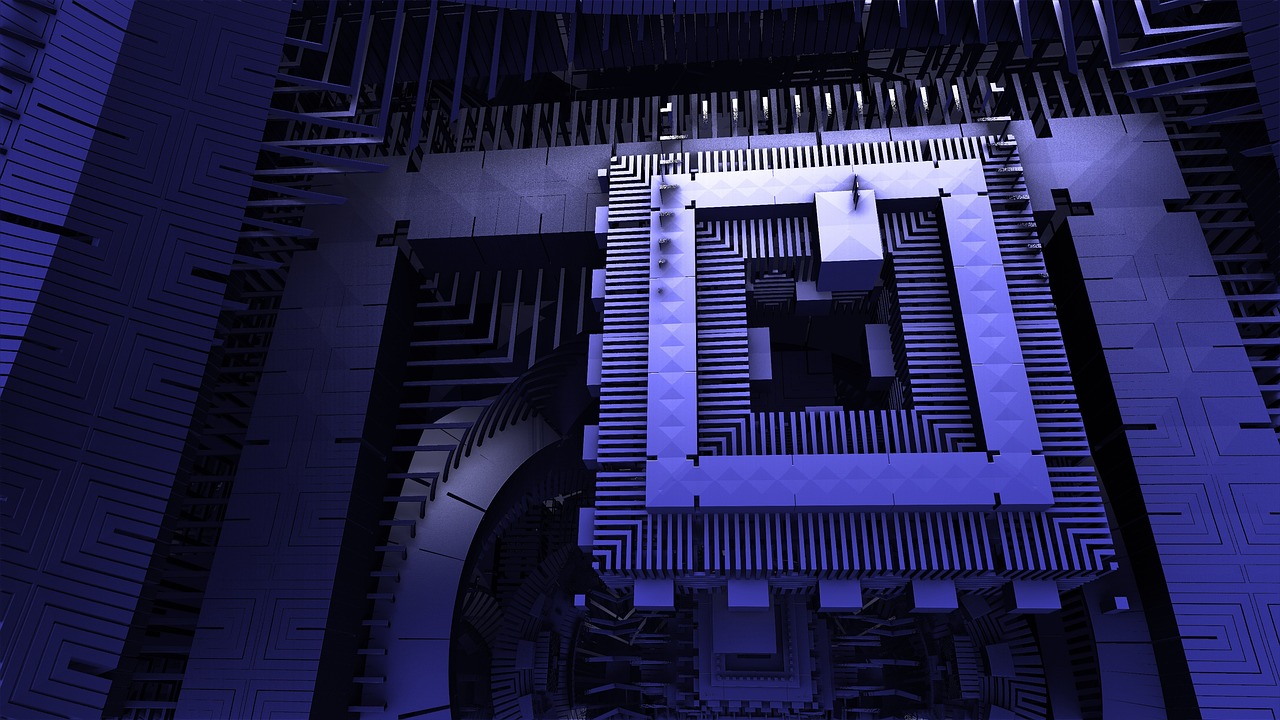
Another way Intel is enhancing 18A is by introducing new technologies called RibbonFET and PowerVia. In simple terms, RibbonFET is a redesigned transistor layout that builds on Intel’s long-used FinFET approach by rotating the ribbon structure.
![]()
Although it may appear to be a small change, it delivers numerous benefits such as improved control of electrical current, lower power leakage, and greater transistor miniaturization, among other advantages. In summary, RibbonFET allows for smaller transistors and thus a higher transistor count which should lead to better performance. Similarly, PowerVia technology moves power delivery to the backside of the chip. This change increases complexity and cost, but Intel insists the advantages justify it.
Adding Larger Elements Like Signal-Carrying Wires
To appreciate why this matters, it helps to first understand how computer chips have traditionally been made. Chips are built layer by layer from the bottom up, beginning with the smallest components (transistors) and then adding larger elements like signal-carrying wires, known as interconnects, and power delivery structures.
Although backside power delivery raises manufacturing costs, Intel says it lowered frontside costs, keeping total 18A production expenses in line with previous chips. Overall, the company claims 18A delivers 15% better performance per watt than the Intel 3 process and increases chip density by 1.3×.